Printed circuit board (PCB) laser depaneling is an effective way for manufacturers to save money and time. Boards often contain sensitive components that can be damaged easily and laser depaneling reduces undue stress on these components and their solder joints. To avoid unnecessary setbacks, be sure to have a proper understanding of the different methods for PCB depaneling.
In this post, we will take a deep dive into the components of laser routing or cutting for PCB depaneling and the key challenges they can solve for manufacturers.
Choosing Laser Routing (Cutting) for PCB Depaneling
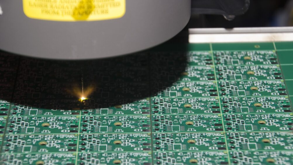
Laser routing, or laser cutting, has become a popular method for depaneling. This process makes no physical contact with board, eliminating the problem of physical stress. Many manufacturers have chosen laser routing as its ideal for flexible, highly sensitive, small PCBs used in the latest wearable technologies.
The two most commonly used lasers for PCB depaneling are CO2 (10.6µm wavelength) and UV (355nm wavelength). The main deciding factor when determining which laser to use is the relative importance of cycle time versus cleanliness of the cut edge.
Selecting the Right Laser Source: Pros & Cons
Determining the right laser source for your PCB depaneling needs should be your first priority. Let’s look at the pros and cons of CO2 vs. UV lasers:
CO2 Lasers:
If cycle time is more important than char, a CO2 laser source is utilized.
- Pros: Fast cut speeds, lower cost per watt than UV, perforated or full cut (see below) option, thicker substrates cut efficiently, and aluminum panels can be processed.
- Cons: More charring on cut edges, larger HAZ, and larger kerf width.
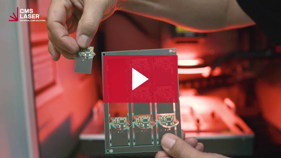
CO2 lasers, which can be used to create full cuts, are more frequently used to make perforated cuts.
Perforated cuts for PCB depaneling leave the “to-be” singulated board attached to the panel but require less force “to-be” separated than other techniques. Using the perforation technique reduces char compared to full cuts and also makes for simpler load and unload of panels and singulated boards from the cutting machine.
An important factor in the perforation technique is the gap between perforations. A larger gap will result in less char on the cut edge but will require more force to separate boards. Perforation strength can be easily adjusted based on specifications.
Additionally, as material thickness increases so does cycle time and amount of charring on cut edges. If panels can be manufactured with V-grooves (or even better “U” grooves”) at cut locations, laser cuts can be made cleaner and faster.
UV Lasers:
Lasers that incorporate UV use “cold” cutting technology. Thermal charring of the edge is more controllable with UV lasers. Thus, if minimizing char is more important than speed, a UV laser is the preferred choice.
- Pros: Extremely clean cuts (medical industry quality), narrow kerf width (due to small spot size), ability to cut copper leads without smearing, low HAZ, and cut edge retains high electrical resistance between layers.
- Cons: Longer cut times than CO2 and more expensive.
When using a UV laser to achieve clean cuts, multiple repetitions of laser scanning are used to singulate the PCBs. Software controls are used to regulate the cut speed, delays, and path sequencing to fine tune the cut quality.
These cuts are a full cut through the entire panel that completely singulate the board.
CMS Laser’s Application Lab can help determine which option is right for your application through our Free Sample Processing.
Improving Cut Accuracy for PCB Depaneling
The accuracy of the cuts made while depaneling PCBs is also important for reducing damage and waste. The challenge is to provide consistent cut placement by ensuring proper alignment of the laser with panel features and components.
The solution to this challenge is a vision system. For PCB depaneling, the vision system locates specific features on the panel (fiducials, “V”-Grooves, circuit shape, or other orientation distinguishing features) and adjusts the cut path accordingly to ensure correct alignment of the cuts to the circuits.
Why Select Laser Depaneling vs. Other Methods
As previously discussed, the laser routing or cutting method is a no-contact process which in turn means the following:
- Can cut any path including curves. Not restricted to straight lines
- No mechanical stress on parts (especially critical for sensitive circuits).
- No need for sharpening or replacing worn blades.
- Software controls that allow for quick and simple changing between different cut patterns.
- Vision systems that can help switch between pre-programmed cut patterns as a new panel is loaded.
- No need for realigning blades or switching mechanical parts between types of panels.
Final Thoughts
Mechanical methods are responsible for various degrees of stress that may ultimately damage the boards. Lasers however, exert no physical stress on the board, reduces the required spacing between circuits, and easily transitions between flex and solid substrates. What is most important to CMS Laser is selecting the right laser system for PCB depaneling that meets client specifications.
Stay tuned for the final post in our three-part series on PCB depaneling as we will discuss a complete systems overview for PCB depaneling and explore the evolution of PCB depaneling with lasers.
Still have questions? Contact CMS Laser to speak with one of our specialist about laser PCB depaneling systems